.png)
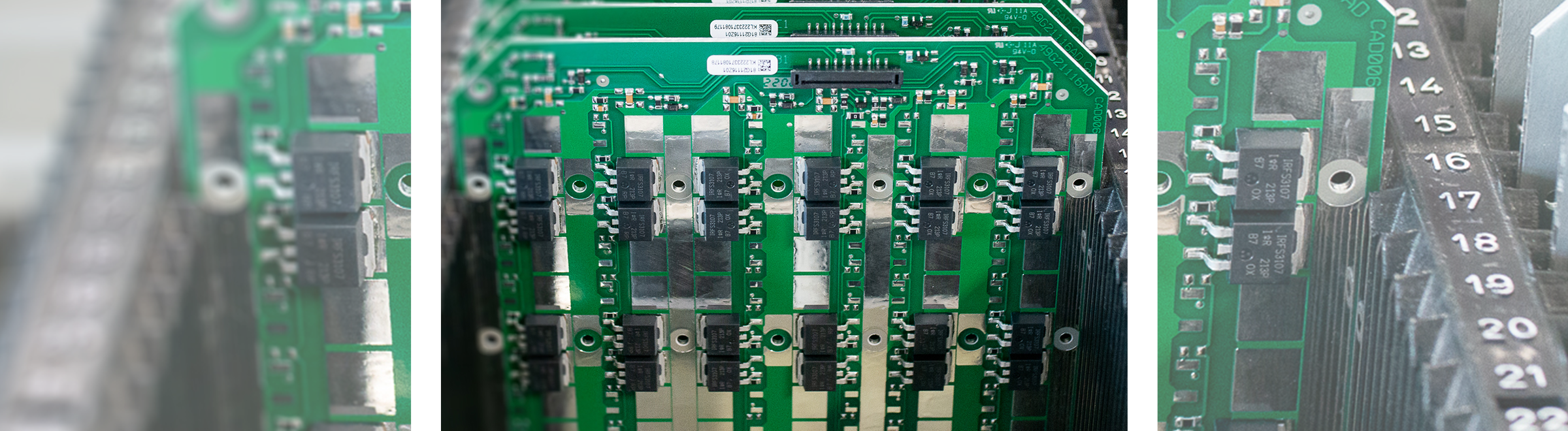
In the past few decades, electronic boards and components have dramatically shrunk in size while increasing in functionality and performance.
This means that very small and high-density packaged electronics boards can be designed and manufactured with today's traditional surface-mounted technology components.
For some applications, our customers' product needs to go beyond traditional surface-mount technology. For example, you need even smaller electronics, or you are looking for electronics that can cope with extremely harsh environmental requirements and special performance or functional needs.
For those special needs, we have built a capability in microelectronics manufacturing that builds electronics with naked chips directly on the board or other carrier substrates. This can be compared to similar manufacturing technology that is used inside an electronics component, such as an integrated circuit. However, we use the chip component directly without the component package.
Microelectronics enables smaller sizes and more robust devices. For example, for products that must withstand high temperatures, harsh environments, high frequency, high power, and vibrations, this service can be the most effective option.
A unique area in our manufacturing - the cleanroom
The stability of our products can only be ensured by maintaining a clean manufacturing environment. We cannot risk any particulate contamination on advanced electronics - even a tiny speck of dust can damage a microchip. Kitron Sweden's special cleanroom environment filters air to high levels. Protective clothing and masks must be worn by all workers to prevent contamination.
Using the latest technology and expertly trained technicians, our electronics assembly cleanrooms and labs exceed the industry's standards for contamination control and cleanroom compliance. Our cleanrooms are designed to maintain low levels of air particulates and control temperature and humidity. They are regularly monitored and inspected to ensure they meet standards.
How does microelectronics work?
In terms of Kitron's services and capabilities, we offer microelectronics services, which include naked chip technology. It is an advanced method of chip-to-substrate connection that eliminates the need for a wire bond. This reduces the overall weight and size of the component, making it easier to install and more reliable. Naked die – as it is also known, is widely used in high-end products such as aerospace, medical, and defence applications. It is becoming increasingly popular in consumer products due to its superior performance and cost savings.
But there are cases where we use die bonding and wire bonding. These are two processes that connect semiconductor devices to a substrate.
Die bonding involves attaching a semiconductor die to a substrate using bonding material. It is performed with specialized equipment in a cleanroom environment to ensure the die is assembled according to tolerances in the bonding process.
Wire bonding, on the other hand, involves making connections between the semiconductor and the substrate with fine wires. At Kitron Sweden, we offer AIuminium and Gold wire bonding services for both fine and heavy wire applications. Our highly trained engineers are skilled at both manual and automated wire bonding processes and can provide the highest quality of service.
The quality of die bonding and wire bonding processes can have a significant impact on the finished product's performance and reliability. Thus, it is essential to ensure that both processes are carried out with the utmost precision and accuracy.
In addition, Kitron also provides ribbon bonding for RF applications. This process is used to connect multiple pins in a single operation, making it ideal for high-frequency electronics. Ribbon bonding is a cost-effective and reliable process that is suitable for both prototyping and production. It is also very versatile, as it can be used with a wide range of materials.
To continue, how can we define hermetic encapsulation? As the name implies, it seals semiconductor components from the environment, protecting them from dust, moisture, and other contaminants. This process involves encapsulating the component in a metal enclosure with a hermetic seal to prevent moisture and other contaminants from entering the package. By encapsulating the component, its performance, and reliability can be greatly improved.
A few more relevant details about microelectronics - we also use plasma cleaning to remove contaminants from surfaces. It works by producing a low-pressure plasma created by applying electrical energy to a gas to break down organic and inorganic molecules on the surface of the material. This process is often used to remove organic contaminants, such as dust and oils, that can affect the performance of the components. Plasma cleaning is a cost-effective and efficient way to maintain clean surfaces in microelectronics.
In the same way as other technologies, microelectronics must also ensure its reliability. It is necessary to perform the testing.
So, we use probe testing, a process utilized in microelectronics to evaluate electrical performance. It involves inspecting the device with a specialized probe that is connected to a testing device. This allows the measurement of a variety of parameters, such as current, voltage, and resistance. Probe testing can be used to identify manufacturing defects, ensure device performance meets specifications, and troubleshoot problems in advance.
Testing the quality of the wire bond can also be done through pull testing. We take a sample and attach it to a microscopic hook to check if the bond is strong enough. The hook then pulls on the connection to measure the bond force. This test allows us to measure if the bond is capable of withstanding any external forces.
To conclude, all of these processes and technologies are used in microelectronics to ensure device performance and reliability. Each process plays an important role in the design and manufacturing process and must be performed with attention to detail to ensure optimal results.
Summary
As technological advancement continues, electronics manufacturers want to produce more without compromising quality. As a result, microelectronics cleanrooms prove valuable.
Kitron is a true partner in manufacturing the most advanced microelectronics products. The unique advantage we offer is our ability to approach service from the customer's perspective, integrating various specialties on-site, balancing cost-benefits and schedules, and managing it all with the highest levels of quality, reliability, and expertise. Our customers can take advantage of the most advanced methods by combining PCBA technology with microelectronics.
Kitron Sweden has provided this unique service for many years. It helps ensure that our customer's products meet the highest quality standards. We strive to remain at the forefront of technology and provide excellent service.