At Kitron, we have been using advanced Automated Optical Inspection (AOI), a key process control in surface mount (SMT) manufacturing that gives us full confidence in the quality of the finished products. But what to do about the cases where we cannot optically see solder connections?
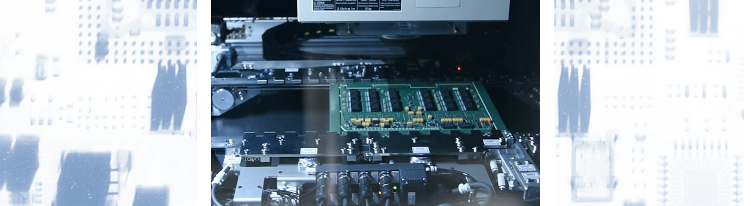
To handle such cases, at Kitron Sweden, we have an advanced in-line 3D X-ray inspection system with a high degree of accuracy. Micro-focus X-ray tubes provide stable flux yielding, better repeatability, and improved call accuracy.
How does it work?
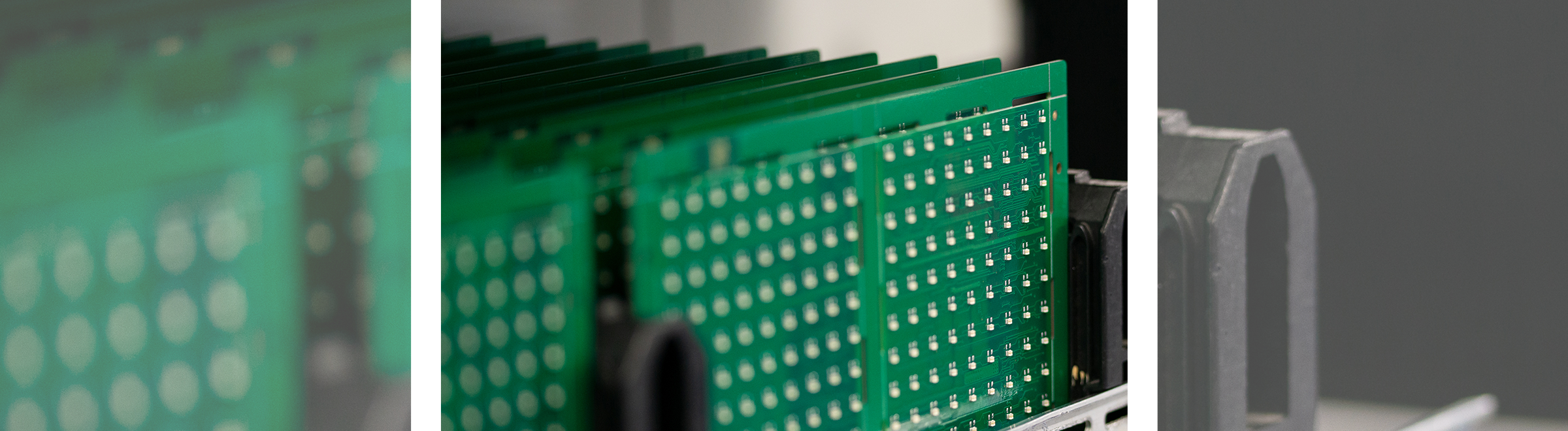
In electronics manufacturing, 3D X-rays are used to inspect the inside of components, assemblies, and printed circuit boards (PCBs). In other words, the object is inspected using X-ray technology to get a first-class 3D image quality.
3D X-ray images can be used to detect defects that may not be visible to the naked eye. The three-dimensional X-ray inspection captures both the top and bottom sides of PCBs within a continuous process. It can also be used to verify the assembly and soldering of components inside the PCB. This technology improves product quality and reduces costs.
3D reconstruction with the X7056-II technology is based on planar computer tomography. For complex overlapping, as is virtually the rule with printed circuit boards assembled on both sides, leveraging the superb three-dimensional inspection possibilities offered by the system makes all significant features sharply visible in clear slice images to enable precise evaluations – even for shadowing by components or on multi-layer boards. This means false calls are effectively prevented while inspection program creation is simplified.
In 3D X-ray inspections, multiple 2D X-ray images are taken from different angles and combined to make a 3D image of the object. Analysis of the resulting image can reveal any defects or anomalies within the object's structure. This type of inspection is more accurate and comprehensive than traditional 2D X-ray inspections and can detect even the smallest of defects. 3D X-ray inspections are used in a variety of industries, as well as at Kitron.
3D X-rays also provide a more detailed view of the PCB and can detect smaller defects. The revolutionary xFastFlow handling concept cuts time for automatically printed circuit board changes down to 4 seconds. Inspection depth and throughput can be optimally adapted to meet individual requirements. In general, it allows more efficient production, as it can be used to quickly detect and address issues that would otherwise cause costly delays.
Different PCBs differ in size, weight, and friction coefficient, among other things. The intelligent printed circuit board transport intelliFLOW takes this into account and automatically determines the optimal travel parameters. As a result, specific products can be handled at optimized times.
The system is available in various speed configurations and can be adapted to customer-specific test strategies by means of two different image acquisition concepts.
Inspecting solder joints for BGAs, QFNs, THTs, LEDs, and LGAs is one of the standard tasks. Additionally, any other solder joints on a PCB can be inspected, whether they are visible or hidden. The 3D planar computed tomography process can also be used to inspect press-fit connectors. During X-ray inspection, there are no AOI-typical reflections and shadows that could influence the inspection. An inspection is carried out by measuring the absorption of different materials of varying densities and thicknesses. The color and gloss level of a surface does not influence X-ray inspection. This makes it possible to detect even the smallest defects. Because of this, X-ray inspection is so precise and reliable, making it an ideal solution for quality control.
Electronic components and assemblies are better quality and more reliable when they're inspected in 3D. 3D X-ray inspections are also faster and more cost effective than traditional 2D X-ray inspections. They can be used to inspect both individual components and entire assemblies in a matter of seconds. This makes them an invaluable tool for the quick and accurate inspection of products.
Added value for our customers
We are proud that our customers can count on us to provide maximum reliability. In-process control with a 3D X-ray can help reduce the chances of misplaced, hidden inaccuracies making assemblies impossible to repair. The most significant benefit is that this is a very cost-effective way to control the highest quality – no guessing about where problems appear if a product fails the test, or doesn’t work. This helps to reduce production costs, as well as shorten the time to market for new products.
Summary
We're confident that Kitron Sweden provides high-quality services to our customers by using 3D X-ray inspection. As a result of it, we can examine the inside of components, assemblies, and printed circuit boards (PCBs). 3D X-ray inspection allows us to detect flaws and defects that can't be seen with standard inspection methods. This technology enables us to detect and prevent problems before they become serious issues, and saves our customers' time and money in the long run. This ensures that our products meet the highest quality standards and keep our customers successful.